CMOS Integrated Circuit Wafer Fabrication & Metrology
End-to-end silicon fabrication of planar pMOSFETs, pn junctions, and MOS capacitors in a Class 100/1000 cleanroom, followed by automated I-V/C-V parameter extraction and failure analysis.
From Bare Silicon to Functional Integrated Circuits
In short: I built working transistors, diodes, and capacitors on a bare silicon wafer by hand, in a real cleanroom, then measured how well they actually worked.
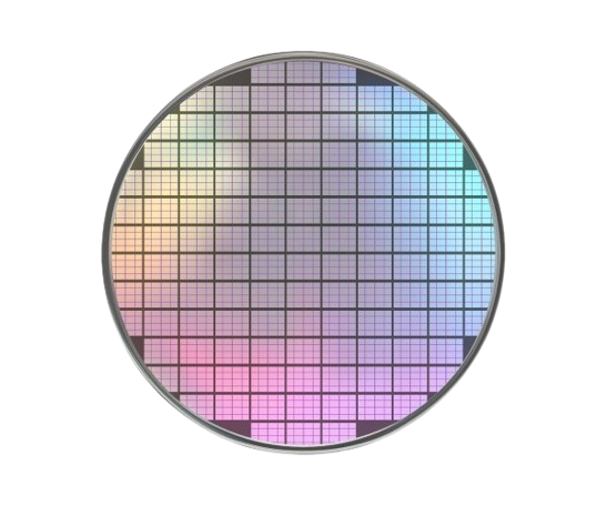
In ECE 444 (Theory and Fabrication of Integrated Circuits) at UIUC, I fabricated a silicon wafer containing planar MOSFETs, lateral BJTs, pn-junction diodes, and MOS capacitors from scratch in a Class 100/1000 cleanroom — the same device types inside every real chip, built one wafer at a time instead of by the billion.
Fabrication used a 5-mask photolithographic process: diffusion, gate oxidation, etching, and aluminum metallization. Afterward I measured every device electrically and compared the results back to the process — where a mask undercut, where diffusion spread sideways more than planned, where parasitic resistance crept in.
Cleanroom Fabrication Process Flow
Every structure on the wafer came from the same five-mask sequence, built up layer by layer:
- Oxidation: RCA clean, then grow a thick field oxide over the whole wafer.
- Mask 1 — Deep p-type wells: Open the mask, etch through the oxide, then diffuse boron in deep (15 min predeposition + 45 min drive-in).
- Mask 2 — Shallow n-type wells: Diffuse phosphorus in shallow, no drive-in, for a sharp junction.
- Mask 3 — Gate oxide: Strip the oxide over the channel, regrow a thin 250 Å dielectric.
- Masks 4 & 5 — Contacts and metal: Open contact vias, evaporate aluminum, pattern it, then sinter in forming gas.
Transconductance & Channel Length Discrepancy () Analysis
In short: the transistor’s real channel is shorter than what I drew in CAD, because dopants and etching both eat sideways into it. Draw the channel too short and the two ends touch underground, killing the transistor.
Dopants diffuse sideways under the gate mask, and the BOE etch undercuts the oxide the same way, so the real (metallurgical) channel length is always shorter than the CAD length: . If that shrinkage ever equals or exceeds the drawn length, the source and drain regions meet underneath the gate — a punch-through short with no gate control left at all.
On my wafer, the shortest device that still worked had , so has to sit somewhere between about and .
I extracted the exact value from a measurement that doesn’t need to know the gate bias or threshold voltage: comparing the saturation transconductance of a long-channel and a short-channel pMOSFET side by side.
The trick: take the ratio of the two devices’ transconductance slopes (). Mobility and oxide capacitance are the same for both devices, so they cancel out of the ratio, leaving an equation with only unknown:
Solving it with the measured data gave — almost exactly the cutoff where devices stopped working. That’s not a coincidence: it’s the whole explanation for why nothing shorter survived.
Diode Forward Characteristics & Ideality Factor ()
In short: a real diode isn’t a perfect diode. Two effects blur its textbook I-V curve, and I had to correct for one of them before the underlying physics was visible.
The base-collector diffused diodes follow the standard junction equation:
Correcting for Series Resistance ()
Plotted against the raw terminal voltage, the ideality factor looks distorted at both ends: leakage dominates at low voltage, and series resistance () chokes off current at high voltage. Neither is the diode’s real behavior.
is fixable: pull it from the linear slope of the forward I-V curve at high current, then subtract its voltage drop back out:
Once corrected, the curve makes sense: climbs from recombination at low bias, levels off around , then drops again at high forward current.
MOS Capacitor - Profiling & Substrate Characterization
In short: sweeping voltage across a tiny capacitor and watching its capacitance change reveals how good the oxide is and how heavily the silicon underneath is doped — without needing to cut the wafer open.
I swept three circular MOS capacitors () from accumulation to inversion to pull out oxide integrity, flatband voltage, and substrate doping:
| Structure | Die Location | [pF] | [pF] | Calculated [pF] | Extracted [V] |
|---|---|---|---|---|---|
| MOSCAP #1 | (2,3) | 51.79 | 49.09 | 941.61 | -10.4 |
| MOSCAP #2 | (2,7) | 52.50 | 39.40 | 157.90 | -16.6 |
| MOSCAP #3 | (2,8) | 52.20 | 42.00 | 214.94 | -12.3 |
Parameter Extraction
At strong inversion, the oxide capacitance and the silicon’s own depletion-layer capacitance act like two capacitors in series (). Solving that for the depletion capacitance gives the maximum depletion width , and from there the substrate’s actual donor concentration :
| Device | Depletion Width [cm] | Extracted [V] | Extracted [] |
|---|---|---|---|
| MOSCAP #1 | -28.3 | ||
| MOSCAP #2 | -27.3 | ||
| MOSCAP #3 | -28.5 |
Dielectric Breakdown Analysis
In short: the oxide on this particular test wafer was almost 6× thicker than intended, and that single fact explains why its breakdown field looked so much weaker than a fresh gate oxide’s should.
Breakdown field is just — voltage where the oxide fails, divided by how thick it is. I compared two ways of getting :
| Method | Oxide Thickness | Breakdown Field [V/cm] |
|---|---|---|
| Dry Oxidation Curves | 250 Å | |
| Measured - Accumulation | 1402 Å |
The measured thickness (1402 Å) is nearly 6× the 250 Å the dry-oxidation growth curve predicted. That gap — native oxide buildup and interface traps on an aged test wafer — is what dragged the breakdown field down from the ~7.2 MV/cm a fresh thermal oxide should hold.
Takeaways
Channel shortening this close to the drawn length ( against a device) is why modern CMOS nodes need self-aligned gates — at this scale, lateral diffusion alone can kill a transistor. Threshold voltages pulled from the MOS capacitors clustered more tightly than the ones extrapolated from FET curves, a reminder that interface traps and contact resistance quietly bias four-terminal parameter extraction.